
Inside the Chip: The Fascinating Journey of Semiconductor Manufacturing – Part 1


Ever wondered how the tiny semiconductor chips inside your smartphone, computer, or car come to life? It’s a story of extraordinary precision, where humble grains of sand are transformed into the powerful brains of our digital world. Imagine constructing a towering skyscraper, layer by layer, with meticulous detail and that could be compared to how a semiconductor chip is built.
Welcome to our comprehensive guide to the fascinating industry. In this series of articles, we’ll explore the world of semiconductors, from their essential manufacturing processes and the current structure of the industry to key terminologies you must know, all aimed at helping you better understand the industry.

In this series, we’ll break down the core steps that turn raw silicon into a functioning chip: wafer manufacturing, oxidation, photolithography, etching, deposition and ion implantation, metal wiring, EDS, and packaging.
For this first installment, we’ll focus on the essential early stages: wafer manufacturing and oxidation. These steps lay the foundation for the entire chip-making process. Let’s take a closer look at where the chip’s journey begins.
Wafer Manufacturing: Laying the Foundation
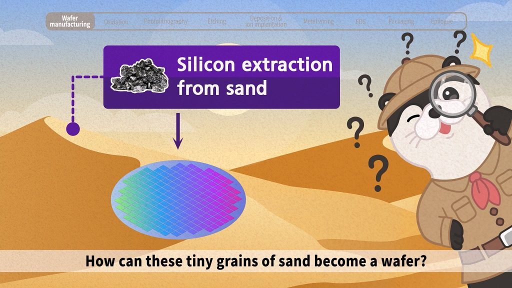
Just like constructing a skyscraper begins with a foundation, semiconductor manufacturing begins with the wafer, a thin, disc-shaped slice primarily made of silicon extracted from sand. This process starts by heating sand until it melts and then purifying and crystallizing it into a silicon ingot. The ingot is sliced into ultra-thin discs known as wafers.


However, these sliced wafers have rough surfaces and may contain defects that can interfere with the precision of circuits that will be laid out onto the chips. To address this, further polishing is needed to smooth the surface of the wafer.
Oxidation: Forming a Protective Shield

Next comes the oxidation step, where oxygen or water vapor is sprayed on the wafer surface to form a uniform oxide film. This layer acts as a crucial protective barrier during later processes and, importantly, prevents electrical current from leaking between circuits. Essentially, the oxide film works as a strong protective shield for the wafer.
With its surface polished and shielded, the wafer is now ready, a blank canvas poised for design. Next, in Part 2, we’ll explore how circuit patterns are etched onto this surface, forming the chip’s essential structure.


